Chapter 6
Direct Digital Imaging
Aim
The aim of this chapter is to provide a comprehensive understanding of direct digital x-ray imaging in dentistry.
Outcome
After reading this chapter the reader should be able to:
-
understand the technology underlying direct digital imaging
-
identify the differences between it and conventional film radiography
-
see the clinical implications of using direct digital sensors.
What is Direct Digital Radiography?
Direct digital radiography involves the acquisition of digital data without an intermediate stage between exposure and image production. This is in contrast to indirect digital radiography (see Chapter 7), which requires an intermediate stage between the exposure of the patient and obtaining the image (i.e. the reading of a phosphor plate).
Direct digital imaging is achieved using a solid-state sensor to detect x-rays. All sensors have the same basic design, with a detection stage and a readout stage, although there are differences between sensors according to manufacturer and their clinical use (intraoral, panoramic or cephalometric radiography).
X-ray Detection
There is a vast array of dental x-ray equipment on the market that uses direct digital technology. Abbreviations such as CCD and CMOS are freely used in manufacturers’ literature. In this section we hope to cast some light on this highly technical subject.
In direct digital imaging, the detection of x-rays may be through either direct or indirect conversion. This is not to be confused with direct or indirect detection but relates to the conversion of the x-rays to an electronic signal. These methods are described in more detail later, but both rely on solid-state materials at some stage in the image production.
Solid-state Materials
All direct digital detectors are solid-state devices; this means that they have no moving or mechanical parts. The device is a solid object, usually comprising electronic circuitry such as diodes and transistors; a good example is computer memory. These components are made from solid-state materials; materials that have properties that can be exploited at the material level, such as being semiconducting or superconducting. Many solid-state materials are crystalline, although amorphous materials (those with no ordered structure) are used in x-ray sensors. The two most commonly used are amorphous silicon (aSi) and amorphous selenium (aSe). These two materials are, however, usually used in completely different ways, with aSe being used for x-ray detection and aSi used for readout.
Indirect Conversion
At the time of writing, the most common technology for x-ray detection uses an indirect conversion method. The term “indirect” relates to the fact that the x-rays, incident on the detector, do not directly induce an electronic signal, but need to go though a secondary process. In this case, the process is the production of light by a scintillator.
X-ray scintillation is the conversion of x-ray photons to visible light photons. It is a well known property of some materials and has been used extensively in medical imaging, both in the phosphor plate in film screen cassettes and in the entrance phosphor on image intensifiers. Common materials used in digital detectors are the rare earth gadolinium oxysulfide (GdO2S2) and caesium iodide (CsI). GdO2S2 is used in its amorphous state (Fig 6-1a) as a light-emitting layer in the sensor sandwich.
CsI can also be used in this way, but newer methods can grow the columnar crystal of CsI directly onto the detector surface (Fig 6-1b). This has significant advantages: the detection layer can be thicker so that more light is produced than with GdO2S2, increasing the efficiency of the sensor; and it has less scatter than an amorphous material, as the crystal structure acts like a light pipe, resulting in theoretically greater detail resolution. Both emit green light that is detected by discrete photosensitive sites to be converted into an electric signal (Fig 6-2).
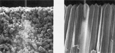
Fig 6-1 Electron microscope images of scintillators used in indirect conversion of x-rays; a) GdO2S2 amorphous structure; b) CsI columnar structure. The amorphous structure of the GdO2S2 and columnar structure of the CsI can be clearly seen. (Courtesy of Varian X-ray Products).
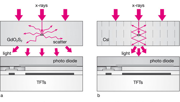
Fig 6-2 Examples of indirect conversions using a scintillator and a thin film transistor (TFT) array; a) GdO2S2 scintillator; b) columnar CsI scintillator.
Direct Conversion
With direct exposure sensors there is no scintillator. Instead, the x-rays are directly converted to a charge in the material through the photoelectric effect. This occurs in both aSi and aSe, although the conversion is not very efficient in the former. Currently, the material of choice for direct conversion is aSe.
X-ray exposure produces a charge (positive and negative) in the selenium, the size of which is proportional to the quantity of x-rays incident upon it. By placing a high voltage (kilovoltage) across the aSe, these charges can be moved to the surface to produce an electric current (Fig 6-3). This current is stored in a matrix of discrete capacitors that can then be read.
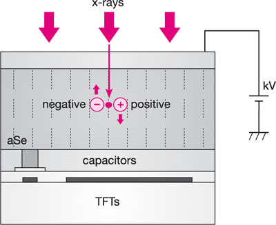
Fig 6-3 Example of direct conversion using an aSe detector: kV = kilovoltage.
Image Readout
In reading out the image data, three parameters need to be recorded: the pixel x position, the pixel y position and the signal intensity at that site. The x and y positions can be acquired either by direct addressing, as with a thin film transistor array (TFT), or by coupled readout, as used in charge-coupled devices (CCDs).
TFT
A thin film transistor (TFT) array is exactly as its name suggests: an array of up to millions of transistors made of silicon on a glass substrate. The transistors are used in conjunction with capacitor or photodiode elements to allow direct addressing of individual charge sites. TFTs can be used with either direct or indirect conversion devices. This technology is also used in liquid crystal displays (LCDs), where each individual transistor is used to control the state of the liquid crystal to allow light to be transmitted. The advantages of the TFT are the ability to address each of the individual transistors for direct readout and that physically large matrices, with many millions of transistors, can be made.
CCD
A charge-coupled device (CCD) is an image sensor consisting of an array of linked, or coupled, light-sensitive capacitors built on an aSi layer. CCDs are generally used with indirect conversion devices, and it is one of the most common technologies used for dental sensors. The image is read out sequentially by shifting an entire readout row of charges down into a readout buffer. When a row is moved into the readout buffer all the rows above are moved down as well. The row number gives the y coordinate. To obtain the x coordinate, the row is sampled by shifting each charge out of the readout buffer into the detection electronics, one element at a time (Fig 6-4).
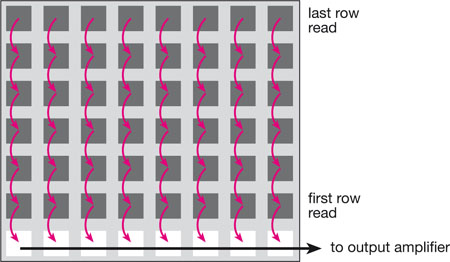
Fig 6-4 Schematic of the readout process of a CCD sensor.
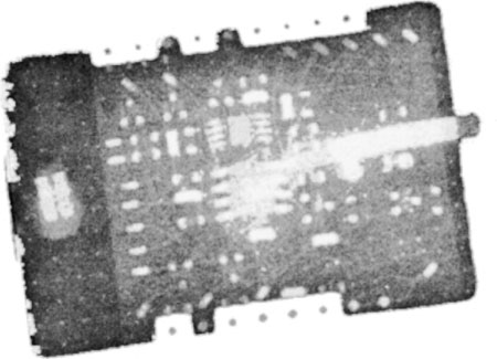
This is the same technology as used in digital cameras. One disadvantage of a CCD is that the sensor can only be made quite small, up to a maximum of about 4 cm, although it is possible to get around this limitation by joining detectors together. The advantages are that CCDs are relatively cheap and have a near 100% fill factor. A radiograph showing the construction of a CCD detector is shown in Fig 6-5.
Stay updated, free dental videos. Join our Telegram channel
VIDEdental - Online dental courses