3 Instrumental Techniques for Study of Orthodontic Materials
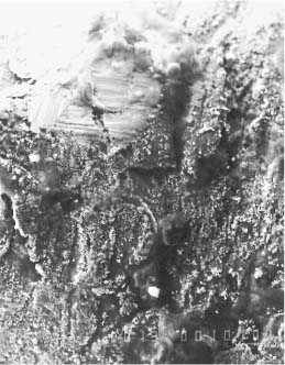
Secondary electron image (SEM) of a retrieved stainless steel orthodontic wire covered by intraoral integuments
X-ray Fluorescence (XRF) Spectrometry
X-ray Fluorescence (XRF) Microanalysis
Electron Probe Microanalysis (EPMA)
Auger Electron Spectroscopy (AES)
Scanning Auger Microprobe (SAM)
X-ray Photoelectron Spectroscopy (XPS)
Secondary Ion Mass Spectrometry (SIMS)
Fourier Transform Infrared Spectroscopy (FTIR)
Multi-technique Characterization
Differential Scanning Calorimetry (DSC)
Introduction
Current advances in analytical instrumentation offer powerful tools for the study of orthodontic biomaterials and for the characterization of tissue-material interactions. The introduction of computer-controlled systems has greatly expanded the use of various spectroscopic methods in the field, providing important information for the elemental, molecular, and structural characteristics of biomaterials. Moreover, a variety of techniques have been developed for studying material surfaces and interfaces, which dominate the expression of the biological response to biomaterial properties in vivo.
This chapter will discuss the analytical techniques of X-ray fluorescence spectroscopy and microanalysis, X-ray diffraction, electron probe microanalysis, Auger electron spectroscopy and scanning Auger microprobe, X-ray photoelectron spectroscopy, secondary ion mass spectrometry, Fourier transform infrared spectroscopy, Raman microspectroscopy, and differential scanning calorimetry. The fundamental principles, experimental procedures, and advantages and limitations of each technique will be presented. Examples of their application to the study of orthodontic materials will be provided.
The objective of this chapter is to present information at a level that is suitable for individuals in orthodontic materials research who are beginning to use these techniques or who need to communicate with laboratory personnel who operate the instrumentation. Other readers should find this information useful for a better understanding of research articles describing studies that have employed these techniques. More detailed presentations are available in the textbooks and other references listed at the end of this chapter.
Of the various types of spectroscopic methods available in integrated commercial systems, the most common and versatile are X-ray spectroscopy, photoelectron spectroscopy, ion spectroscopy, and vibrational spectroscopy. These techniques are dependent upon the nature of the target’s response to the incident probe. Some of these methods simultaneously provide structural identification images. The depth of analysis obtained with these methods varies from a monolayer fraction (< 0.1 nm) up to many micrometers, according to the type of the radiation probe and the target used. Methods employing particles of high-energy radiation require high-vacuum or ultrahigh-vacuum environments to achieve undisturbed primary beam emission and secondary beam detection and to avoid surface contamination from the atmospheric environment. The use of high-energy probes in a high-vacuum environment has raised important questions about the relevance of these methods in studying hydrated specimens or tissue-biomaterial interfaces. Excessive drying may lead to molecular reorientation phenomena; radiation damage may alter the target composition; ion-induced destructive depth profiling may intermix target elements; and electrostatic charging may result in a severe spectral distribution for insulators. For all these reasons, the complementary use of techniques suitable for analysis of hydrated specimens has been advocated. In the present chapter a review of the spectroscopic methods used in characterization of orthodontic biomaterials is presented, aiming at better understanding the principles, procedures, advantages, and limitations of each one.
X-ray Fluorescence (XRF) Spectrometry
When an atom of an element is bombarded by X-rays of sufficient energy, inner-shell electrons absorb energy and are ejected, producing atomic vacancies; this phenomenon is known as the photoelectric effect. The excited atom then relaxes to the ground state by transition of outer orbital electrons that fill the inner-shell vacancies. Characteristic X-rays are produced that correspond to the atomic energy loss to the excited element and are annotated by the orbital where the original vacancy was created (e.g., Cr Kα). Since the X-rays produced are independent of the chemical environment of the atoms, they are suitable for elemental analysis. X-ray emission may be produced by electron beams, charged particles, X-rays, or radioactive isotopes.
The most practical energy source for X-ray fluorescence (XRF) spectrometry is an X-ray tube. Tubes do not require high vacuum or conductive samples as do electron beams, nor accelerators as does particle-induced X-ray emission, and with a single source many elements can be excited efficiently, unlike isotopic sources where more than one source is required. Selection of the X-ray tube anode material should be made so that the characteristic lines emitted by the anode are close to, but always of higher energy than, the absorption energies of the elements of interest, without creating spectral interferences. In quantitative standardless applications where monochromatic radiation is required, filters can be used with the primary radiation from the X-ray tube so that essentially only characteristic lines of the tube anode are transmitted.
Elemental identification in XRF spectrometry is accomplished by spectrometers that resolve the spectral lines emitted into separate components. There are two types of spectrometers that are available: (1) in wavelength-dispersive spectrometry (WDS) the X-rays emitted are dispersed into specific wavelengths by the mechanical movement of analyzing crystals attached to a goniometer and detected by proportional or scintillation counters; (2) in energy-dispersive spectrometry (EDS), semiconductors are used to create signals proportional to the X-ray energy. The WDS systems demonstrate higher resolution, higher-sensitivity detection, and higher counting rates than the EDS ones. However, owing to single-channel detection they are slow, and because of the goniometer arrangement they are very sensitive to topographical features. EDS is very fast because of multichannel detection and provides simultaneous multi-element analysis capability, although not all elements can be determined in every sample under the same conditions. The voltage of the X-ray tube is critical for the excitation of the elements in both WDS and EDS, and should be set higher than the absorption edge of the elements probed. The range of accelerating voltage for WDS is 0–100 keV, while for EDS the range is 0–40 keV. The tube current affects only the X-ray photon flux and thus the count rate. XRF spectrometers can operate with the sample chamber kept at atmospheric conditions, under vacuum or under helium. Generally, for detection of X-rays below 5 keV, vacuum or helium purging is required.
XRF spectrometry can be applied nondestructively to the analysis of solid samples of various forms (bulk, powders, and briquets), liquids, thin films, and filtered aerosol samples (Fig. 3.1). The technique can detect elements with atomic number Z > 11. Oxygen and fluorine can be semi-quantitatively measured using special crystals or detectors. Detection limits for bulk determinations are typically from a few ppm up to a few tens of ppm, dependent on the energy used and the sample composition. For thin films, detection limits may reach 100 ng/cm2.
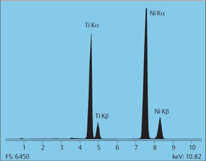
Fig. 3.1 Energy-dispersive X-ray fluorescence spectrum of a nickel-titanium orthodontic wire
The depth of analysis in XRF varies from few micrometers to a millimeter or more, depending on the X-ray energy used and the nature of the target. A growing application of XRF is in measuring film thickness and composition of coatings. Several techniques have been developed, such as the substrate intensity attenuation method, the coating intensity method, and the various intensity ratio methods for rapid on-line measurement of film thickness. Results with submicrometer accuracy can be obtained with the use of appropriate sets of standards.
X-ray Fluorescence (XRF) Microanalysis
Developments in the field of X-ray capillary waveguides allow microfocusing of X-ray beams at areas approximately 100 μm in diameter with the aid of an incident light optical microscope, thus introducing energy-dispersive XRF spectometry in the field of microanalysis. The area of analysis is identified optically and is rapidly analyzed without the need for specimen preparation, dehydration, and application of a conductive coating. Samples may be analyzed in atmospheric conditions, under low vacuum, or under helium purging. Although the spatial resolution of XRF microanalysis is poor and the depth of analysis greater compared with electron probe microanalysis, the flexibility of the technique and the minimal requirements for sample preparation offer unique advantages in studying hydrated specimens.
X-ray Diffraction (XRD)
X-ray diffraction (XRD), which is used to study the crystal structures of materials and related matters, is one of the major traditional laboratory tools employed in materials science. Figure 3.2 shows a beam of parallel X-rays that are incident upon atomic planes at the surface of a crystalline material. If the difference in path length for X-rays reflected from adjacent planes is an integral number of wavelengths, these reflected X-rays will be in phase and produce a strong signal at some detector. In order for this constructive interference to occur, the interplanar spacing (d), angle of incidence (θ) and X-ray wavelength (λ) must be related by Bragg’s law:

The diffraction angle (2θ) is the angle between the incident and transmitted X-ray beams. The number of wavelengths in the path length difference is designated by n, which is termed the order of diffraction.
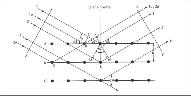
Fig. 3.2 Diffraction (reflection) of a set of parallel X-rays at the surface planes of a crystalline material. (From Cullity, 1978)
In the customary XRD methodology for orthodontic materials, nearly monochromatic characteristic X-rays, such as Cu Ka radiation, are used. As described earlier, characteristic X-rays are generated when the accelerating voltage in the X-ray tube is sufficiently high (typically > 10 kV) that the electrons, created by passing a current (typically > 10 mA) through a filament, have the necessary energy to knock out core electrons from the K level (innermost shell) of the target metal. The most likely transitions are for electrons from the L shell to fill the vacancies in the K shell, with the creation of Kα X-rays. However, the K shell vacancies can also be filled by electrons from the M shell, which results in the emission of Kβ X-rays. (Transitions from other shells to the K shell can also occur, but these do not make a significant contribution to the beam from the X-ray tube.) An appropriate filter material or a crystal monochromator is used to greatly reduce the intensity of the Kβ X-rays, so that nearly monochromatic Kα X-rays are used for XRD analyses. Details of operation of the X-ray tube and the use of filters and monochromators are provided in textbooks on X-ray diffraction.
In the usual experiments, a polycrystalline specimen in flat plate form or a polycrystalline powder specimen is analyzed. In XRD studies of archwires, a series of parallel wire segments may be placed in contact to obtain an acceptable specimen for the diffractometer. Figure 3.3 shows that the diffracted X-rays from an atomic plane in a polycrystalline powder specimen form a cone when the powder contains a very large number of randomly oriented crystals. The diffracted X-rays from a powder specimen may be detected with a Debye-Scherrer camera that contains film or with a diffract-ometer. Plate-shaped archwire specimens used with the diffractometer will not have randomly oriented crystals (grains) because of the preferred crystallographic orientation resulting from the wire drawing process, as described in Chapter 4.
Figure 3.4 is an XRD pattern for 40 8C Copper Ni-Ti (Chapter 4) obtained with Cu Kα radiation, which is representative of results for the poly-crystalline archwire alloys. The diffracted X-ray intensity is plotted on the vertical axis as a function of the diffraction angle (2θ) on the horizontal axis. The XRD peaks for the two phases present have been indexed by comparing their positions to those in the polycrystalline powder standards for austenitic (18–899) and marten-site (35–1281) NiTi, published by the International Center for Diffraction Data (ICDD) (Swarth-more, PA, USA).
The method is illustrated in Table 3.1, which presents the information provided in the ICDD standard for bcc (modified CsCl structure) austenitic NiTi: the positions (d) of the observed XRD peaks (hkl) and their relative intensities (I). The peak positions are given as values of the interplanar spacings because the diffraction angles (2θ) will depend upon the type of X-ray tube chosen. Tubes with many different metal targets are available, so that an investigator can select the wavelength of the characteristic radiation, such as Cu Kα, Mo Kα or W Lα. Table 3.1 shows the successive steps for the use of Bragg’s law to locate the 2θ positions of the peaks for the standard when Cu Kα radiation (λ = 1.5418 Å or 0.15418 nm) is employed. The relative peak intensities are normalized to the intensity for the strongest peak, which is assigned a value of 100.
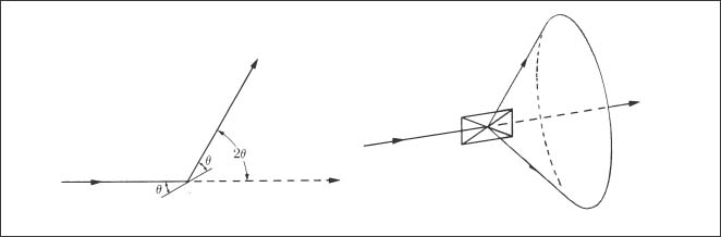
Fig. 3.3 Formation of a cone of X-rays diffracted from a powder specimen containing a large number of randomly oriented crystals. (From Cullity, 1978)
Fig. 3.4 X-ray diffraction pattern for 40 °C Copper Ni-Ti obtained at room temperature. (An abstract describing this study is found in Brantley et al, 1998).
Differences in observed relative intensities for the peaks in Figure 3.4, compared to values for the ICDD standard in Table 3.1, are due to the strong 110 preferred orientation of the austenitic NiTi in the archwire. Differences in the observed peak positions (2θ values or the corresponding interplanar spacings), compared to the ICDD standard, arise from incorporation of solute atom species (copper and chromium) in the crystal structure of the phase being analyzed.
For some materials the surface atomic planes giving rise to the XRD peaks can be under a state of uniform residual elastic strain. For uniform tensile strain, the interplanar spacing (d) will be increased, and consideration of Bragg’s law shows that the diffraction angle (2θ) for the reflection from these planes is decreased; the diffraction angles are increased if the surface planes are under uniform compressive strain. Substantial peak broadening is often observed in XRD patterns from archwires owing to residual plastic deformation arising from the wire processing sequence, as described in Chapter 4. The peak broadening arises because the complex pattern of permanent deformation involves both tensile and compressive strains.
The hkl column in Table 3.1 represents the Miller crystallographic indices for the particular sets of atomic planes that give rise to the observed peaks for austenitic NiTi. While a detailed discussion of the structure factor for Xray diffraction is beyond the scope of this chapter, it can be noted that for each crystal structure (other than simple cubic) only certain sets of parallel atomic planes yield constructive interference of the reflected monochromatic Xray beam. This series or pattern of observed XRD peaks is unique for the particular crystal structure (analogous to a “fingerprint”). When two materials, such as iron and nickel, have the same crystal structure (fcc in this case, as described in Chapter 1), the pattern of the XRD peaks is the same, although the peak positions (2θ values) differ because of the different lattice parameters.
The hkl indices are the reciprocals of the intercepts of the given atomic plane on the three crystallographic axes (conventionally termed x, y and z) for the unit cell. An index of zero means that the atomic plane is parallel to the corresponding axis of the unit cell. For example, the 310 peak in Table 3.1 is for a series of planes that intersect the x-axis at one-third of a unit (lattice parameter) and the y-axis at one unit from the origin. Because these planes are parallel to the z-axis, the z-intercept is considered to be infinity, which yields a reciprocal value of zero for the Miller index. For martensitic NiTi, which has a monoclinic crystal structure (Chapter 1), a negative crystal-lographic index, designated by a bar over the number, is shown for the 1 1 reflecting plane in Figure 3.4. The peak positions and intensities in ICDD standard 35–1281 for martensitic NiTi are shown in Table 3.2. A negative crystallo-graphic index for a crystal plane indicates that the intercept is on the corresponding negative axis with respect to the origin for the unit cell.
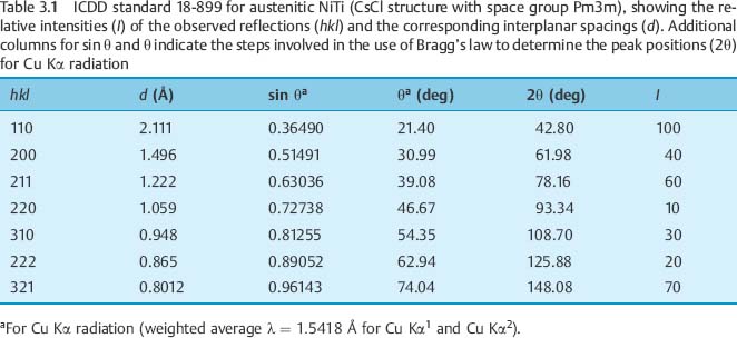
For materials containing more than one phase, such as 40 °C Copper NiTi in Figure 3.4 or some stainless steel archwires, as discussed in Chapter 4, the XRD pattern will contain the series of peaks for each phase. Some phases, such as chromium carbide in stainless steel archwires, may not have significant XRD peaks because of their composition and structure or because the amount of the phase in the micro-structure is too small. For the analysis of an unknown material by X-ray diffraction, computerized search programs that are available with modern diffractometers are used to compare the strongest observed peaks with the library of ICDD standards. Indexing the peaks for a multiple-phase material where no information is available about the microstructure can be a very difficult task. Common problems are overlapping peaks from different phases and the existence of a preferred orientation that greatly alters the relative intensities of peaks from those in the ICDD standards.
X-ray diffraction is inherently a near-surface analytical technique, since the depth of penetration of the X-ray beam is typically no greater than 50 μm and frequently much less for the metals of usual interest. Consequently, caution is necessary when interpreting the results of XRD experiments, since the near-surface structure of a material may differ significantly from the bulk structure. While such an experiment is generally very difficult to conduct, the safest procedure is to perform a series of XRD analyses on specimens from which known thicknesses of surface layers have been removed.
Most research articles in the orthodontic materials literature involving the use of X-ray diffraction have focused on archwire alloys. Recent studies have shown the applicability of X-ray diffraction to the identification of phases in zirconia ceramic brackets (Chapter 7) and to the characterization of changes in tooth enamel under clinically important conditions. Fluoroapatite formation in enamel due to fluoride release from glass ionomer cement, the analysis of enamel lesions to confirm whether fluoride was incorporated during remineralization, and the effect of gel applications on enamel crystallinity have been investigated. These topics will be discussed further in Chapters 6 and 11.
Electron Probe Microanalysis (EPMA)
In electron probe microanalysis (EPMA) an electron beam accelerated at 10–30 keV is microfocused on a small area (10 nm to 1 μm in diameter), and specimen microvolumes are excited by scanning the beam over the target. The inner-shell electrons of target atoms are ionized, and upon relaxation they emit either X-rays from a one-stage transition, as described before, or undergo radiationless two-stage transitions producing Auger electrons. X-ray emission decreases in favor of Auger emission as the atomic number decreases, and this is the main reason why Auger electron spectroscopy is more sensitive in light-element analysis. When X-ray emission occurs, the emitted X-rays can be detected by WDS or EDS, providing information about the elemental composition of material microregions. The depth of analysis depends on the accelerating voltage and the target properties. In EDS the depth is approximately 1 μm, while in WDS, which usually operates at higher accelerating voltage, the depth may exceed 5 μm. The lateral resolution is somewhat larger owing to diffuse scattering of the incident electrons. The detection limits are 0.1% by weight for EDS and 0.01% by weight for WDS. EPMA requires conductive specimens to avoid electrostatic charging. For the study of insulators, conductive coatings should be applied.
Modern EPMA systems are coupled to scanning (SEM), conventional transmission (CTEM) or scanning transmission (STEM) electron microscopes. Thermionic SEMs can be equipped with both WDS and EDS systems. Low-pressure and environmental SEMs, CTEMs and STEMs are mostly compatible with EDS. EPMA offers the following analysis modes: (a) point analysis, where a spectrum at a selected point is taken; (b) line scan analysis, where the elemental gradients along a linear direction are measured; and (c) area scan analysis, where the elemental distribution in the form of elemental mapping is traced. Imaging and analysis in EPMA are performed by detecting various electron signals emerging from secondary emitted electrons, backscattered electrons, and characteristic X-rays. However, since the sample volumes contributing to these signals are different, care should be taken about the correct interpretation of the results (Fig. 3.5). Secondary electrons, providing the conventional SEM images, originate from the uppermost few nanometers. Backscattered electron images, especially from the inelastically scattered fraction, originate from a depth of hundreds of nanometers, while characteristic X-rays originate from a depth of a micrometer or more. Since the atomic number contrast of backscattered electron detectors is stronger than that achieved with the secondary electron detectors, backscattered electron images are preferred for assigning elemental distributions, especially in multiple-phase specimens. The use of backscattered electron images is most important when analyzing features with sharp edges (e.g., interfaces), because detection of the forward-scattered electrons by the secondary electron detector produces image flaring. This distortion is minimized in backscattered electron images, and clear interfaces are obtained.
As in XRF spectrometry, WDS demonstrates superior resolution to that of EDS, better sensitivity for low-atomic-number element analysis (Z < 10), and lower detection limits by a factor of 10–100; superior elemental distribution images (elemental mapping) will be obtained. However, WDS is more sensitive to topographical features owing to beam defocusing, needs higher vacuum and higher beam currents than EDS, and is considered more destructive to organic materials. For quantitative analysis of specimens with unknown composition, EDS offers the advantage of rapid multi-element detection. Nevertheless, WDS systems are the spectrometers of choice for resolving overlapping peaks or for the quantitative analysis of major and minor constituents. Both spectrometer types are sensitive for elements with Z ≥ 5. The most common artifacts in qualitative analysis by EDS are the sum peaks, the escape peaks and the internal fluorescence peaks. Sum peaks are recorded at the low-energy region from major spectral components due to coincident detection. Escape peaks are produced from the photon detection process in the [Si (Li)] detector, where sometimes silicon is in an excited state emitting X-rays at ~1.74 keV. Internal fluorescence peaks may arise from the thin silicon layer in front of the detector. Care should be taken for peaks over 15 keV, which usually appear at low intensity because the efficiency of the detector at the high-energy region is reduced, since some X-rays can penetrate through the detector. In WDS analysis the main problem is the production of a series of peaks from the diffraction orders of the same element that appear at different angles (harmonic peaks). In the low-energy region (< 2 keV) peak shifting may occur, depending on the chemical state of the element in the sample.
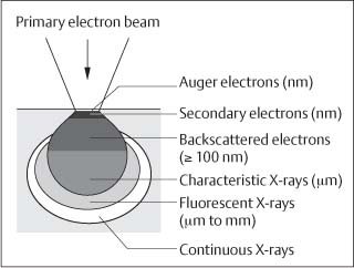
Fig. 3.5 The different depths of various information obtained from a specimen subjected to electron beam irradiation
The most important advantage of EPMA is elemental mapping, which provides qualitative and quantitative information on the area distribution of the elements in a specimen (Fig. 3.6). There are two types of elemental mapping. In conventional or analog dot-mapping, the X-ray signal from the spectrometer is synchronized with the image display, so that an elemental distribution image of modulated brightness is recorded. The concentration variations are denoted by differences in the area density of the dots. Owing to li/>
Stay updated, free dental videos. Join our Telegram channel
VIDEdental - Online dental courses