Fig. 4.1
The principle behind XPS: an incoming X-ray excites the atoms and as result emits a photoelectron (Courtesy of Jose J. Chavez, Ph.D. Candidate – Department of Electrical Engineering, The University of Texas at El Paso)
The kinetic energy (KE) of the emitted electrons is measured using a spectrometer. From the kinetic energy, the element-specific binding energy (BE) is obtained, which is easily calculated by subtracting the KE and spectrometer working function (φ) from the incoming X-ray energy (hν), a calculation most often performed directly by the instrument software. The resulting data is presented as a graph where the electron binding energy (eV) is plotted as a function of intensity (counts), i.e., the XPS spectrum. Two examples of XPS spectra are presented in Fig. 4.2 for commercially pure titanium (a) and titanium coated with a thin layer of hydroxyapatite, HA (b).
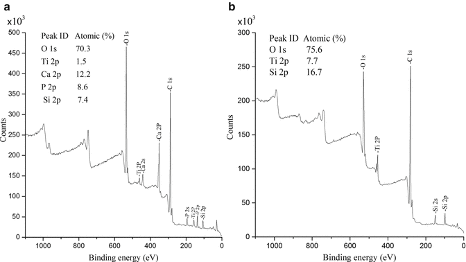
Fig. 4.2
Typical XPS survey spectra for a titanium implant (a) and a hydroxyapatite (HA)-coated titanium implant (b)
The peaks in the XPS spectra represent the different types of photoelectrons ejected from the sample and are labeled according to their quantum numbers. The labeling is usually following the scheme xyz, where x is the principal quantum number (1, 2, 3…), y is the orbital (s, p, d, f, etc.), and z describes the differences in spin angular momentum, which results in some peaks that are split into two. For example, values of z for p orbitals are 1/2 and 3/2, while for d orbitals they are 3/2 and 5/2. XPS is a surface-sensitive technique; however, there is always a penetration depth of the signal, which is dependent on the kinetic energy of the photoelectrons. The depth of analysis is determined by the attenuation length of the electrons and is dependent on the element being analyzed and is in the range of 3–10 nm. The spatial resolution is, however, much less and often in the order of 3 μm2. All XPS analyses are performed under ultrahigh vacuum (UHV) range of 10−8 to 10−10 mbar. The low pressure is needed to reduce scattering of the photoelectrons and to avoid surface contamination from the surrounding air. The samples analyzed need to be carefully handled to prevent contamination, and storage in, for example, plastic bags should be avoided. With the exception for careful handling, most dry solid samples can be directly analyzed without any other pretreatments. Besides for direct surface compositional measurements, XPS can also be used for depth profiling. If the emitted electrons are detected at some angle to the normal, the information depth is decreased, something often related to as angle resolved XPS (ARXPS). In addition to ARXPS, surface material can be removed from the sample within the spectrometer by the use of ion sputtering; hence, deeper depths can be analyzed.
Implant materials are often characterized by XPS since it gives details including:
-
Chemical composition of the surface
-
Presence of undesired contaminants
-
The thickness of possibly present layers such as oxides or additional coatings, for example, hydroxyapatite coatings on titanium
It should be noted that carbon contaminants always are present when analyzing, for example, titanium implants due to adsorption from the surrounding air (see Fig. 4.2). Such detection can be avoided to some extent by the use of surface sputtering. XPS can be considered as the gold standard for chemical characterization of implants.
AES
Auger electron spectroscopy (AES) shares many similarities with XPS when it comes to the actual material properties that can be measured; however, the working principle is somewhat different (see Fig. 4.3) [1].
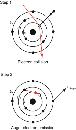
Fig. 4.3
An illustration of the sequences occurring in Auger spectroscopy. Step 1, an electron from the incoming beam kicks out an electron (secondary electron) from an atom in the sample leaving an electron hole. Step 2, an electron from a higher-energy shell fills the hole through an internal transition, and a second electron, named Auger electron, is emitted and detected (Source: http://commons.wikimedia.org/wiki/File:Auger_Process.svg)
In AES, incoming electrons are used to eject core electrons from the sample, often referred to as secondary electrons. When the secondary electrons are replaced within the material, through an internal transition by another electron positioned in a higher energy level, another electron is emitted from the sample due to the first law of thermodynamics, i.e., the conservation of energy. This second emitted electron is termed an Auger electron. The kinetic energy of the Auger electron is element specific and is plotted as a function of intensity. The notation used in AES is different from the XPS. In AES three electrons need to be accounted for, and an Auger electron can, for example, be written as L2M5M5, which means that a secondary electron from the L2 energy level (sometimes also referred to as an energy shell) is kicked out and replaced by an electron from the M5 energy level. A second electron from the M5 energy is emitted, which is the one being measured. Sometimes, the subscripts are excluded leaving LMM as a common notation for an Auger electron. AES bares many similarities to XPS, both being surface-sensitive techniques; however, there are strengths and weaknesses of each technique. Both techniques require the presence of UHV, which to some extent limits the flexibility regarding sample preparations. In AES, difficulties arising from charging effects are more cumbersome, resulting in difficulties in analyzing nonconducting samples, including implants made of ceramics and polymers. The quantification, i.e., surface composition determinations, is less accurate using AES. The lower sensitivity in AES is due to the coexistence of several different internal processes within the atoms resulting in competitive signals. The Auger electrons carry less information about the chemical nature of the samples compared to the photoelectrons analyzed in XPS. It is, for example, not possible to detect the oxidation state of the atoms using AES. The big advantage with AES lies in the high spatial resolution, being less than 10 nm in today’s instruments. Through the combination with scanning electron microscopy (SEM) in the same instrument, it is possible to both visualize surface features down to a few nm as well as have them surface analyzed, a technique coined scanning Auger microscopy (SAM). This possibility is of advantage, for example, when samples are inhomogeneous. For standard characterization of implants, AES is not as frequently used as XPS, which is a combination of availability and the acquired information that is desired. Most often, an implant is chemically homogeneous throughout its surface, and information about what elements that are present, in what concentration, and to some extent their chemical nature is desired; hence, XPS is the preferred choice over AES. However, the ongoing developments implementing nanostructured implant surfaces should cause higher attention toward AES.
SIMS
Stay updated, free dental videos. Join our Telegram channel
VIDEdental - Online dental courses


